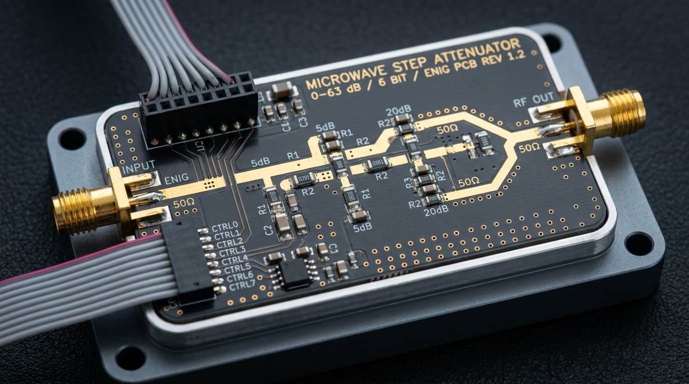
Device Topology & Electromagnetic Behavior
A passive network offering adjustable signal reduction (0 to 30 dB or 0 to 60 dB in 1 dB steps). Utilizes mechanically actuated resistive vanes in waveguide/coaxial cavities or switched thin-film attenuator stages with minimal phase variation across the tuning range.
Rogers RO4350B or RT/duroid® 6002 for phase stability across temperature.
- Balanced symmetrical cell layout to equalize phase delay between reference and attenuated paths.
- Gold-plated contact fingers for low contact resistance and repeatability.
Design, 3D EM Simulation & Handoff for Variable Attenuator (Passive Step / Rotary)
We provide turnkey synthesis, multi-frequency full-wave simulation, and fabrication-ready packaging for the Variable Attenuator (Passive Step / Rotary).
1. 3D Full-Wave FEM Modeling
Complete Ansys HFSS 3D CAD modeling with true edge-launch SMA or SMP connectors, via fence stitching, and adaptive mesh refinement down to ΔS < 0.007.
2. Sensitivity & Tolerance Sweeps
Monte Carlo statistical analysis over copper etching tolerances (±15 µm) and substrate permittivity variations to guarantee first-pass high-yield manufacturing.
3. Manufacturing Handoff
Delivery of verified simulation models, parameterized layout geometries, and photolithography-compliant Gerber RS-274X fabrication packages.
More in Signal Routing & Attenuation
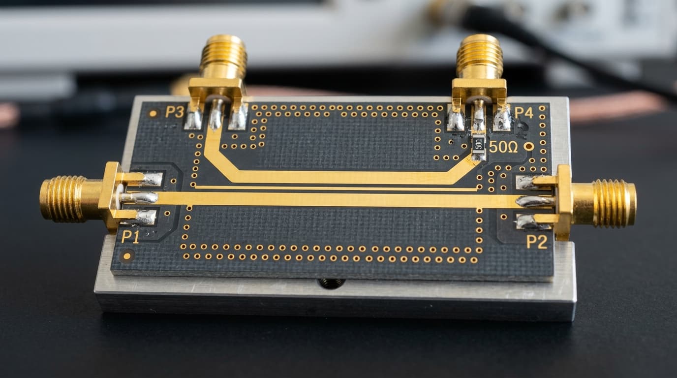
Directional Coupler (Edge-Coupled)
Samples forward RF power with high directivity and minimal mainline loss.
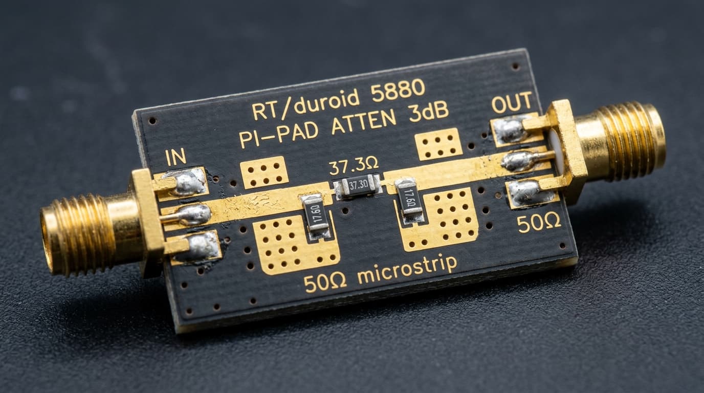
Fixed Attenuator Pad (Pi / T)
Precision resistive attenuation pad for dynamic range leveling and VSWR buffering.
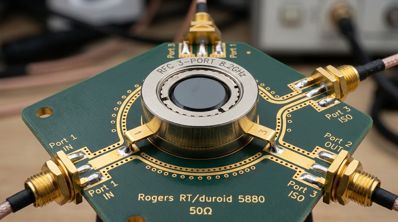
RF Circulator (3-Port Ferromagnetic)
Ferromagnetic non-reciprocal junction routing RF signals in a uniflow circular sequence.
Initiate Design & 3D EM Simulation Scope for Variable Attenuator (Passive Step / Rotary)
Submit your operational frequency, bandwidth, power handling, and target substrate stackup. Our electromagnetic engineers will deliver a verified feasibility audit within 48 hours.
Initiate Project Scope & NDA
We treat client intellectual property with military-grade rigor. Prior to receiving proprietary disclosure files, patent drafts, or trade secret geometries, we execute standard bilateral NDAs.
Bilateral NDA Standard
Mutual non-disclosure executed before file transmission.
Isolated On-Prem Compute
Simulations run on dedicated air-gapped workstations.
Clean Room Protocol
Full audit trail for IP litigation and patent defense.